from: https://rhye.org/post/stm32-with-opencm3-2-spi-and-dma/
이전 섹션 에서는 대체 기능을 다루고 UART를 통해 로그 콘솔을 구성했습니다. 이번에는 에서 사용할 수 있는 SPI 주변 장치를 살펴보고 STM32F0이를 사용하여 데이터를 일부 시프트 레지스터로 빠르게 이동한 다음 DMA를 사용하여 주 CPU에서 해당 전송을 오프로드하는 방법을 시연합니다. 여기에 관련된 다른 IC가 있기 때문에 이전의 간단한 브레이크아웃 대신 이 MIDI 릴레이 보드를 데모 조각으로 사용합니다.
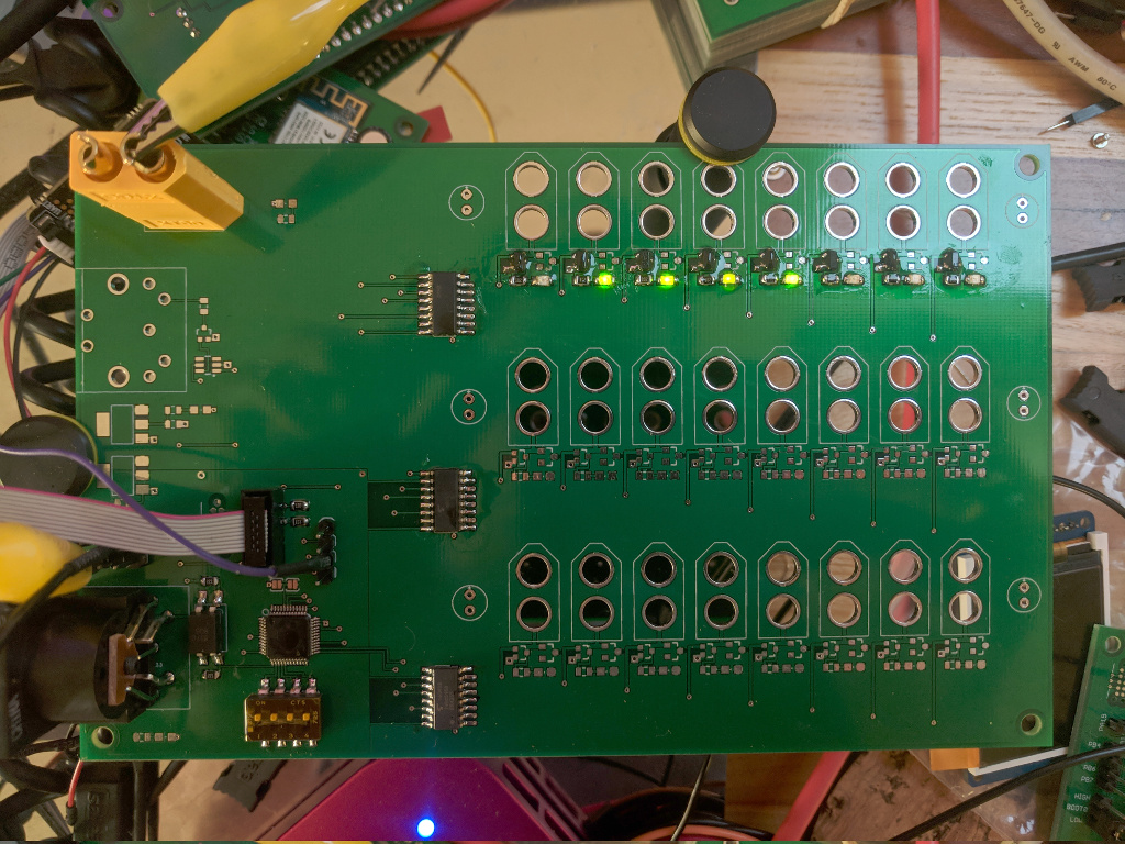
MIDI 솔레노이드 제어 보드(진행 중인 작업).
여기에서 관심 있는 IC는 가운데 아래에 있는 시프트 레지스터 행으로, 각 IC는 각 솔레노이드 연결 지점으로 8개의 FET를 구동하는 역할을 합니다. 이 예에서는 8의 첫 번째 행만 채웠지만 설명하기에 충분합니다. IC STM32F070, SWD 헤더 및 uart 브레이크아웃은 보드의 왼쪽 하단 모서리에서 볼 수 있습니다. 익숙하지 않은 사용자를 위해 시프트 레지스터를 사용하면 직렬 데이터를 가져와 병렬 출력으로 변환할 수 있습니다. 이 IC는 74HC595 모델로 별도의 시프트 및 저장 레지스터가 있는 8비트 시프트 레지스터입니다. 하지만 거기에 데이터를 어떻게 가져오나요? 데이터시트에서 제어 입력을 조작할 때 동작을 정의하는 이 표를 찾을 수 있습니다.
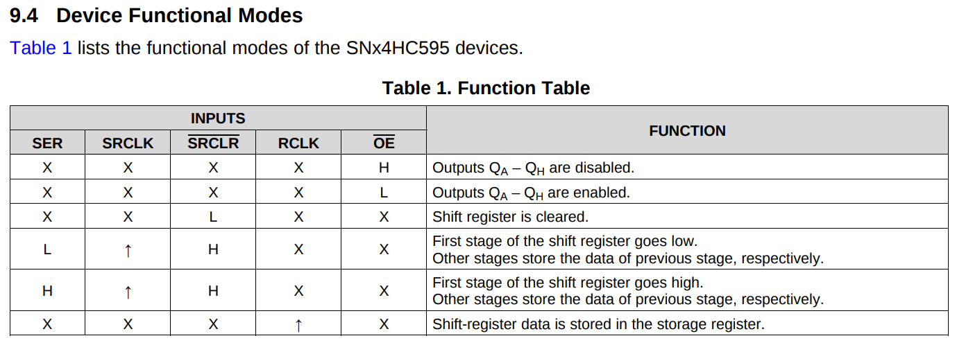
595 시프트 레지스터의 기능 설명
따라서 데이터를 이동하기 위해 순환 SRCLK하고 각 상승 에지에서 데이터가 SER이동 레지스터로 이동하고 현재 이동 레지스터에 있는 모든 데이터가 하나씩 이동됩니다. 이것을 반복하여 원하는 만큼의 데이터를 로드하면 라인을 RCLK로우에서 하이로 클럭하여 시프트 레지스터의 데이터를 스토리지 레지스터로 이동하여 출력에서 볼 수 있도록 할 수 있습니다.
이제 이를 구동하기 위해 우리는 전송하려는 각 바이트를 조심스럽게 가져오고 그 안의 각 비트를 따라 반복하는 메서드를 작성할 수 SER 있습니다 SRCLK. 정확히 같은 일을 하는 주변 장치에서: SPI!
직렬 주변기기 인터페이스
SPI 프로토콜은 일반적으로 4개의 신호로 구성된 간단한 통신 인터페이스입니다.
- MOSI(마스터 아웃 슬레이브 인)
- MISO(마스터 인 슬레이브 아웃)
- SCK(직렬 클럭)
- SS(슬레이브 선택)
UART와 달리 이 프로토콜에는 클록 신호가 있습니다. 결과적으로 양측이 각 비트를 래치할 시기를 정확하게 알 수 있기 때문에 SPI 버스를 훨씬 더 빠른 속도로 작동할 수 있습니다. UART와 마찬가지로 듀플렉스입니다. MOSI 및 MISO 라인은 각각 단방향이며 둘 다 동일한 클록 펄스 동안 데이터를 전송할 수 있습니다. 그러나 SPI는 또한 동일한 MISO 및 MOSI 라인에서 여러 슬레이브(더 복잡한 설정에서는 여러 마스터)를 허용합니다. 슬레이브가 의도하지 않은 데이터를 읽거나 쓰는 것을 방지하기 위해 슬레이브 선택 신호를 사용하여 주소 지정되는 칩을 식별합니다. 특히 SS 신호는 액티브 로우입니다. 이는 SPI MOSI, SCK 및 SS 라인을 사용하여 시프트 레지스터의 SER, SRCLK 및 RCLK 라인에 완벽하게 매핑할 수 있음을 의미합니다. 이 정보를 사용하여 다음과 같이 회로도에 코드화할 수 있습니다.
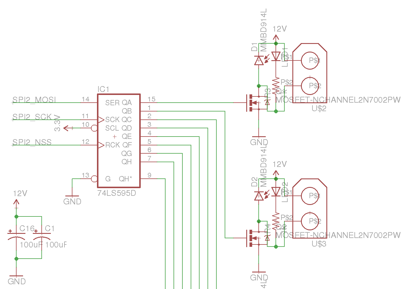
시프트 레지스터 구동을 위한 SPI 연결. 추가 595에는 동일한 SCK 및 NSS 신호가 공급되지만 QH* -> SER로 연결됩니다.
이제 SPI 핀을 시프트 레지스터에 매핑했으므로(이 경우 PB12-PB15 및 SPI2 주변 장치 사용) SPI 주변 장치를 통해 데이터를 보낼 준비를 위해 초기화 작업을 시작할 수 있습니다.
|
1 2 3 4 5 6 7 8 9 10 11 12 13 14 15 16 17 18 19 20 21 22 23 24 25 26 27 28 29 30 31 32 33 34 35 36 37 38 39 40 41 42 43 44 45 46 47 48 49 50 51 52 53 54 |
void spi_setup() { // Enable clock for SPI2 peripheral rcc_periph_clock_enable(RCC_SPI2); // Configure GPIOB, AF0: SCK = PB13, MISO = PB14, MOSI = PB15 gpio_mode_setup(GPIOB, GPIO_MODE_AF, GPIO_PUPD_NONE, GPIO13 | GPIO14 | GPIO15); gpio_set_af(GPIOB, GPIO_AF0, GPIO13 | GPIO14 | GPIO15); // We will be manually controlling the SS pin here, so set it as a normal output gpio_mode_setup(GPIOB, GPIO_MODE_OUTPUT, GPIO_PUPD_NONE, GPIO12); // SS is active low, so pull it high for now gpio_set(GPIOB, GPIO12); // Reset our peripheral spi_reset(SPI2); // Set main SPI settings: // - The datasheet for the 74HC595 specifies a max frequency at 4.5V of // 25MHz, but since we're running at 3.3V we'll instead use a 12MHz // clock, or 1/4 of our main clock speed. // - Set the clock polarity to be zero at idle // - Set the clock phase to trigger on the rising edge, as per datasheet // - Send the most significant bit (MSB) first spi_init_master( SPI2, SPI_CR1_BAUDRATE_FPCLK_DIV_4, SPI_CR1_CPOL_CLK_TO_0_WHEN_IDLE, SPI_CR1_CPHA_CLK_TRANSITION_1, SPI_CR1_MSBFIRST ); // Since we are manually managing the SS line, we need to move it to // software control here. spi_enable_software_slave_management(SPI2); // We also need to set the value of NSS high, so that our SPI peripheral // doesn't think it is itself in slave mode. spi_set_nss_high(SPI2); // The terminology around directionality can be a little confusing here - // unidirectional mode means that this is the only chip initiating // transfers, not that it will ignore any incoming data on the MISO pin. // Enabling duplex is required to read data back however. spi_set_unidirectional_mode(SPI2); // We're using 8 bit, not 16 bit, transfers spi_set_data_size(SPI2, SPI_CR2_DS_8BIT); // Enable the peripheral spi_enable(SPI2); } |
이제 SPI 주변 장치가 데이터를 전송할 준비가 되었습니다. 작업을 더 쉽게 하기 위해 SPI 버스를 통해 주어진 양의 데이터를 전송하는 간단한 도우미 메서드를 만들어 보겠습니다.
|
1 2 3 4 5 6 7 8 9 10 11 12 13 14 15 16 17 18 19 20 21 22 23 24 25 26 27 |
void spi_transfer(uint8_t tx_count, uint8_t *tx_data) { // Pull CS low to select target. In our case, this just pulls the register // clock low so that we can lock in the new data at the end of the // transfer. gpio_clear(GPIOB, GPIO12); // For each byte of data we want to transmit for (uint8_t i = 0; i < tx_count; i++) { // Wait for the peripheral to become ready to transmit (transmit buffer // empty flag set) while (!(SPI_SR(SPI2) & SPI_SR_TXE)); // Place the next data in the data register for transmission SPI_DR8(SPI2) = tx_data[i]; } // Putting data into the SPI_DR register doesn't block - it will start // sending the data asynchronously with the main CPU. To make sure that the // data is finished sending before we pull the register clock high again, // we wait here until the busy flag is cleared on the SPI peripheral. while (SPI_SR(SPI2) & SPI_SR_BSY); // Bring the SS pin high again to latch the new data gpio_set(GPIOB, GPIO12); } |
이제 우리는 SPI를 통해 시프트 레지스터로 데이터를 쉽게 클럭아웃할 수 있어야 합니다. 이를 테스트하기 위해 지난 시간의 기본 루프를 업데이트해 보겠습니다.
|
1 2 3 4 5 6 7 8 9 10 11 12 13 14 15 16 17 |
int main() { // Clock, UART, etc setup // [...] // Initialize our SPI peripheral spi_setup(); // Make a very simple count up display using our 8 LEDs uint8_t i = 0; while (1) { i++; spi_transfer(1, &i); delay(1000); } } |
시프트 레지스터 출력
완벽합니다. 천천히 세고 있음을 알 수 있습니다. 자, 이것은 분명히 SPI의 상당히 작은 응용 프로그램입니다. 여기서 전송할 비트는 8비트뿐입니다(완전히 채워진 보드의 경우 24비트). 이 데이터를 푸시하는 데 정말 극소 시간이 걸립니다. 그러나 이동할 데이터가 많은 경우(예: 화면에 푸시해야 하는 비트맵 데이터) 해당 데이터를 메모리에서 SPI 버스로 이동하는 데 걸리는 시간이 문제가 될 수 있습니다. 보낼 모든 데이터를 반복하고 SPI 데이터 레지스터로 하나씩 이동하면 다른 이벤트를 처리하거나 다음 프레임을 그리기 시작하는 데 시간이 낭비됩니다. 메모리에서 주변 장치로 데이터를 이동하는 것과 같은 간단한 작업을 어떻게든 오프로드할 수 있다면 좋지 않을까요?
직접 메모리 액세스
DMA 컨트롤러를 사용하면 메인 프로세서에서 특정 유형의 데이터 셔플링을 오프로드하여 비즈니스를 계속할 수 있습니다. STM32F0 시리즈에서 컨트롤러를 사용하여 주변 장치에서 메모리로 또는 메모리에서 주변 장치로 두 주변 장치 간에 데이터를 이동할 수 있습니다. 이 예에서는 이를 사용하여 메모리에서 SPI 주변 장치로 데이터를 복사하여 시프트 레지스터로 보낼 수 있습니다. 각 DMA 컨트롤러에는 여러 채널이 있으며 이러한 채널은 모두 특정 주변 장치 기능에 바인딩됩니다. STM32F0 시리즈 데이터시트를 살펴보면 어떤 채널이 어떤 주변 장치에 매핑되는지 보여주는 표를 찾을 수 있습니다.
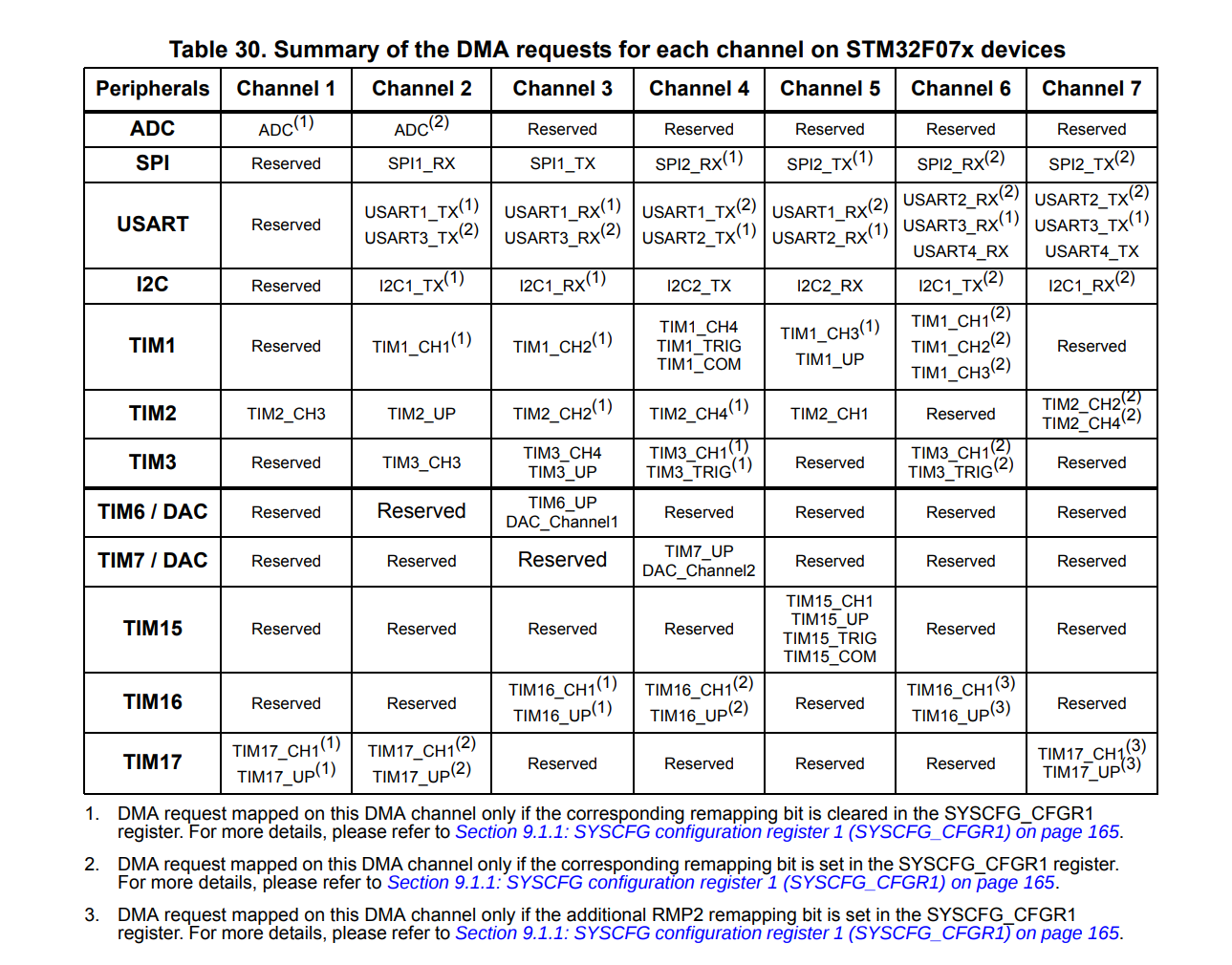
STM32F070 MCU용 DMA 채널 매핑
이를 바탕으로 SPI2에서 데이터를 전송하려면 DMA 채널 5를 사용해야 한다는 것을 알 수 있습니다. 이제 DMA 컨트롤러 구성을 시작하겠습니다.
|
1 2 3 4 5 6 7 8 9 10 11 12 13 14 15 16 17 18 19 20 21 22 23 24 25 26 27 28 29 30 31 32 33 |
void dma_init() { // Enable DMA clock rcc_periph_clock_enable(RCC_DMA1); // In order to use SPI2_TX, we need DMA 1 Channel 5 dma_channel_reset(DMA1, DMA_CHANNEL5); // SPI2 data register as output dma_set_peripheral_address(DMA1, DMA_CHANNEL5, (uint32_t)&SPI2_DR); // We will be using system memory as the source data dma_set_read_from_memory(DMA1, DMA_CHANNEL5); // Memory increment mode needs to be turned on, so that if we're sending // multiple bytes the DMA controller actually sends a series of bytes, // instead of the same byte multiple times. dma_enable_memory_increment_mode(DMA1, DMA_CHANNEL5); // Contrarily, the peripheral does not need to be incremented - the SPI // data register doesn't move around as we write to it. dma_disable_peripheral_increment_mode(DMA1, DMA_CHANNEL5); // We want to use 8 bit transfers dma_set_peripheral_size(DMA1, DMA_CHANNEL5, DMA_CCR_PSIZE_8BIT); dma_set_memory_size(DMA1, DMA_CHANNEL5, DMA_CCR_MSIZE_8BIT); // We don't have any other DMA transfers going, but if we did we can use // priorities to try to ensure time-critical transfers are not interrupted // by others. In this case, it is alone. dma_set_priority(DMA1, DMA_CHANNEL5, DMA_CCR_PL_LOW); // Since we need to pull the register clock high after the transfer is // complete, enable transfer complete interrupts. dma_enable_transfer_complete_interrupt(DMA1, DMA_CHANNEL5); // We also need to enable the relevant interrupt in the interrupt // controller, and assign it a priority. nvic_set_priority(NVIC_DMA1_CHANNEL4_5_IRQ, 0); nvic_enable_irq(NVIC_DMA1_CHANNEL4_5_IRQ); } |
이제 우리의 DMA 컨트롤러는 메모리에서 SPI2의 전송 버퍼로 데이터를 푸시하도록 모두 설정되었습니다. 그러나 설정에서 소스 메모리 위치나 전송하는 데이터의 양을 지정하지 않았음에 유의하십시오. 이제 이에 대한 방법을 추가하겠습니다.
|
1 2 3 4 5 6 7 8 9 10 11 12 13 14 15 16 17 18 19 20 |
void dma_start(void *data, size_t data_size) { // Note - manipulating the memory address/size of the DMA controller cannot // be done while the channel is enabled. Ensure any previous transfer has // completed and the channel is disabled before you start another transfer. // Tell the DMA controller to start reading memory data from this address dma_set_memory_address(DMA1, DMA_CHANNEL5, (uint32_t)data); // Configure the number of bytes to transfer dma_set_number_of_data(DMA1, DMA_CHANNEL5, data_size); // Enable the DMA channel. dma_enable_channel(DMA1, DMA_CHANNEL5); // Since we're manually controlling our register clock, move it low now gpio_clear(GPIOB, GPIO12); // Finally, enable SPI DMA transmit. This call is what actually starts the // DMA transfer. spi_enable_tx_dma(SPI2); } |
그러나 이것은 프로세스의 절반에 불과합니다. 우리는 또한 DMA 전송의 종료 조건을 처리해야 하므로 레지스터 클록을 다시 높게 이동하여 데이터를 래치할 수 있습니다. 이를 위해 DMA 채널에 대한 인터럽트 핸들러를 구현해야 합니다. DMA 채널 4와 5는 동일한 ISR을 사용하므로 dma1_channel4_5_isr지금 구현해 보겠습니다.
|
1 2 3 4 5 6 7 8 9 10 11 12 13 14 15 16 17 18 19 20 21 22 |
void dma1_channel4_5_isr() { // Check that we got triggered because the transfer is complete, by // checking the Transfer Complete Interrupt Flag if (dma_get_interrupt_flag(DMA1, DMA_CHANNEL5, DMA_TCIF)) { // If that is why we're here, clear the flag for next time dma_clear_interrupt_flags(DMA1, DMA_CHANNEL5, DMA_TCIF); // Like the non-dma version, we don't want to latch the register clock // until the transfer is actually complete, so wait til the busy flag // is clear while (SPI_SR(SPI2) & SPI_SR_BSY); // Turn our DMA channel back off, in preparation of the next transfer spi_disable_tx_dma(SPI2); dma_disable_channel(DMA1, DMA_CHANNEL5); // Bring the register clock high to latch the transferred data gpio_set(GPIOB, GPIO12); } } |
모두 연결하고 DMA 전송이 일반 CPU 작업과 분리되어 있음을 보여주기 위해 DMA 전송을 시작한 다음 즉시 USART를 통해 일부 텍스트를 작성해 보겠습니다.
|
1 2 3 4 5 6 7 8 9 10 11 12 13 14 15 16 17 18 19 20 21 22 23 24 25 26 27 |
int main() { // Setup clock, serial, spi, etc // [...] // Initialize the DMA controller dma_init(); // Allocate a nice big slab of data uint8_t data[1024]; for (int i = 0; i < 1024; i++) { data[i] = i; } // Begin a DMA transfer using that data dma_start(data, 1024); // Immediately start printing some text to our console printf("Concurrent DMA and USART!\n"); while (true) { // Nothing } return 0; } |
이제 로직 분석기로 보드의 UART 및 SPI 라인을 탭하면 실제로 SPI 및 UART 데이터를 동시에 전송하고 있음을 관찰할 수 있습니다.
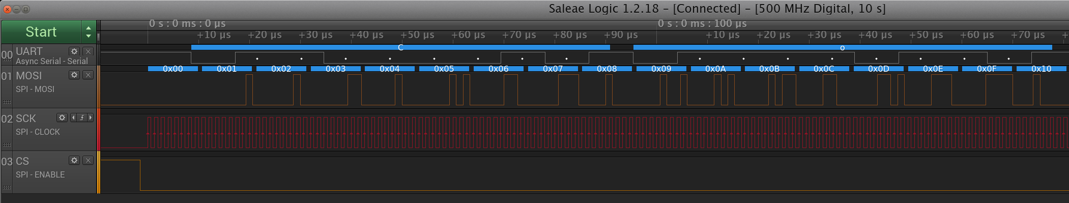
SPI 버스 및 UART TX 추적
성공! 메인 실행 스레드가 USART를 통해 데이터를 전송하는 동안 DMA 컨트롤러가 백그라운드에서 킬로바이트의 데이터를 전송하기 시작했음을 알 수 있습니다. DMA는 프로세서와 동일한 메모리 및 주변 장치 버스를 공유하여 여전히 제한적이므로 둘 다 버스 충돌이 있는 경우 여전히 협상해야 하지만 이러한 방식으로 더 간단한 주변 장치 작업을 오프로드하는 강력한 도구입니다. 원형 DMA 및 “절반 전송 완료” 인터럽트를 활용하여 이중 버퍼링 비디오 데이터 bv 푸시와 같은 보다 복잡한 DMA 작업을 수행할 수도 있습니다.
평소와 같이 이 게시물의 코드는 Github 에서 사용할 수 있습니다 .
CANBus에 대한 이 시리즈의 다음 게시물은 여기에서 찾을 수 있습니다.